- 您现在的位置:买卖IC网 > Sheet目录1997 > ICS843002AKI-41LF (IDT, Integrated Device Technology Inc)IC SYNTHESIZER LVPECL 32-VFQFPN
ICS843002I-41
700MHZ, FEMTOCLOCK VCXO BASED SONET/SDH JITTER ATTENUATOR
IDT / ICS VCXO BASED SONET/SDH JITTER ATTENUATOR
3
ICS843002AKI-41 REV. B
APRIL 7, 2009
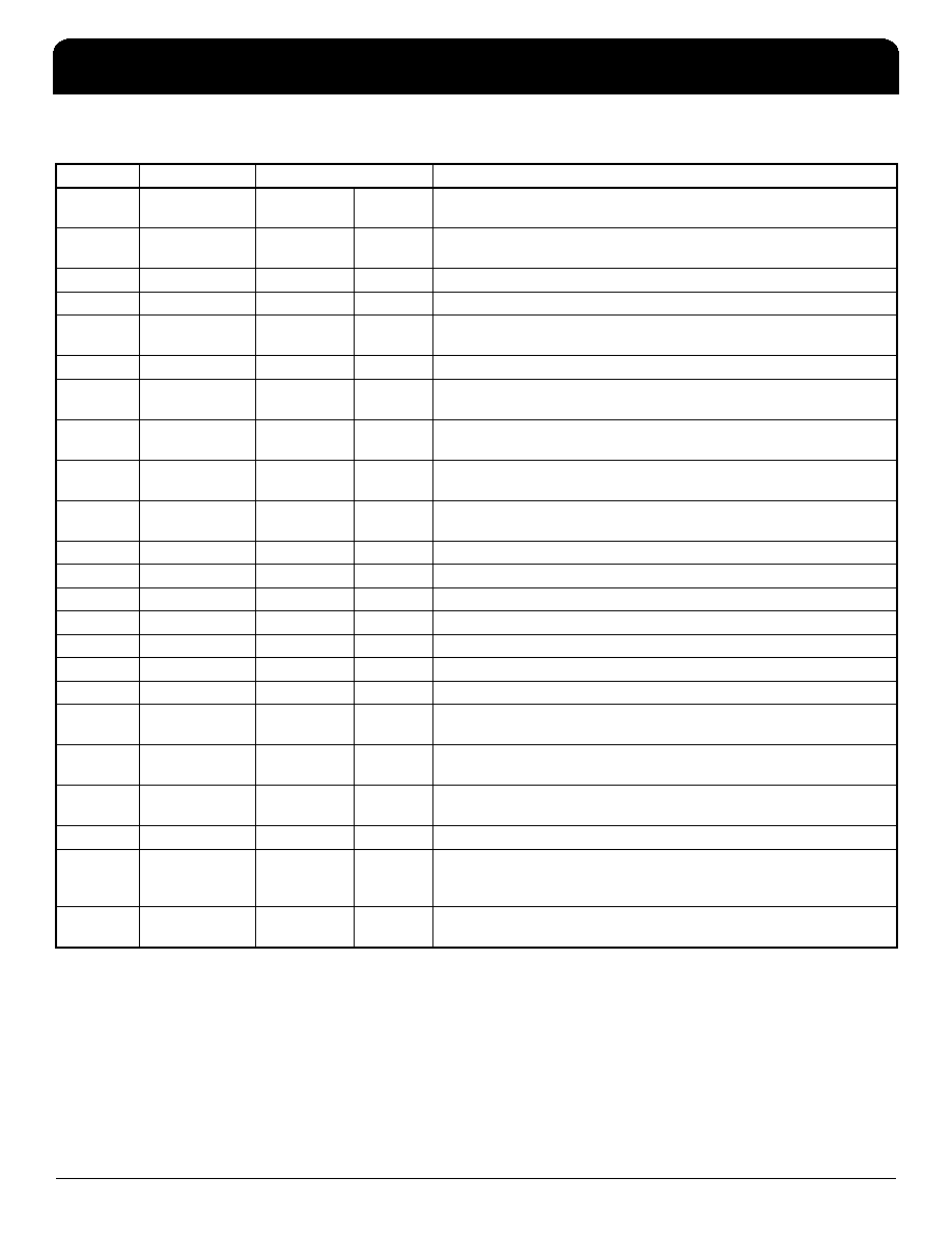
Table 1. Pin Descriptions
NOTE: Pullup and Pulldown refer to internal input resistors. See Table 2, Pin Characteristics, for typical values.
Number
Name
Type
Description
1, 2
LF1, LF0
Analog
Input/Output
Loop filter connection node pins.
3
ISET
Analog
Input/Output
Charge pump current setting pin.
4VCC
Power
Core power supply pin.
5
CLK0
Input
Pulldown
Non-inverting differential clock input.
6nCLK0
Input
Pullup
Pulldown
Inverting differential clock input. VCC/2 bias voltage when left floating.
7
CLK_SEL
Input
Pulldown
Input clock select. LVCMOS/LVTTL interface levels. See Table 3A.
8
QA_SEL2
Input
Pulldown
Output divider control for QA/nQA LVPECL outputs.
LVCMOS/LVTTL interface levels.See Table 3C.
9,
10
QA_SEL1,
QA_SEL0
Input
Pullup
Output divider control for QA/nQA LVPECL outputs.
LVCMOS/LVTTL interface levels.See Table 3C.
11
QB_SEL2
Input
Pulldown
Output divider control for QB/nQB LVPECL outputs.
LVCMOS/LVTTL interface levels.See Table 3C.
12,
13
QB_SEL1,
QB_SEL0
Input
Pullup
Output divider control for QB/nQB LVPECL outputs.
LVCMOS/LVTTL interface levels.See Table 3C.
14
VCCA
Power
Analog supply pin.
15, 16
QA, nQA
Output
Differential clock output pair. LVPECL interface levels.
17, 27
VEE
Power
Negative supply pins.
18, 19
QB, nQB
Output
Differential clock output pair. LVPECL interface levels.
20
VCCO_LVPECL
Power
Output supply pin for LVPECL outputs.
21
VCCO_LVCMOS
Power
Output supply pin for LVCMOS/LVTTL outputs.
22
nc
Unused
No connect.
23
LOR1
Output
Alarm output, loss of reference for CLK1/nCLK1.
LVCMOS/LVTTL interface levels.
24
LOR0
Output
Alarm output, loss of reference for CLK0/nCLK0.
LVCMOS/LVTTL interface levels.
25
nCLK1
Input
Pullup
Pulldown
Inverting differential clock input. VCC/2 bias voltage when left floating.
26
CLK1
Input
Pulldown
Non-inverting differential clock input.
28,
29,
30
R_SEL0,
R_SEL1,
R_SEL2
Input
Pulldown
Input divider selection. LVCMOS/LVTTL interface levels. See Table 3B.
31,
32
XTAL_OUT,
XTAL_IN
Input
Crystal oscillator interface. The XTAL_IN is the input.
XTAL_OUT is the output.
发布紧急采购,3分钟左右您将得到回复。
相关PDF资料
ICS843004AG-02LF
IC SYNTHESIZER LVPECL 24-TSSOP
ICS843004AGI-04LF
IC SYNTHESIZER LVPECL 24-TSSOP
ICS843021AGLFT
IC CLK GENERATOR LVPECL 8-TSSOP
ICS843022AGLF
IC CLK GENERATOR LVPECL 8-TSSOP
ICS843023AGLF
IC CLK GENERATOR LVPECL 8-TSSOP
ICS843031AG-01LF
IC CLK GENERATOR LVPECL 8-TSSOP
ICS843081AGI-01LF
IC CLK MULTIPLIER LVPECL 8-TSSOP
ICS8430AYI-61LF
IC SYNTHESIZER LVPECL 32-LQFP
相关代理商/技术参数
ICS843002AKI-41LFT
功能描述:IC SYNTHESIZER LVPECL 32-VFQFPN RoHS:是 类别:集成电路 (IC) >> 时钟/计时 - 时钟发生器,PLL,频率合成器 系列:HiPerClockS™, FemtoClock™ 标准包装:27 系列:Precision Edge® 类型:频率合成器 PLL:是 输入:PECL,晶体 输出:PECL 电路数:1 比率 - 输入:输出:1:1 差分 - 输入:输出:无/是 频率 - 最大:800MHz 除法器/乘法器:是/无 电源电压:3.135 V ~ 5.25 V 工作温度:0°C ~ 85°C 安装类型:表面贴装 封装/外壳:28-SOIC(0.295",7.50mm 宽) 供应商设备封装:28-SOIC 包装:管件
ICS843002AKI-41T
制造商:Integrated Device Technology Inc 功能描述:IC SYNTHESIZER LVPECL 32VFQFN
ICS843002AKI-72LF
功能描述:IC SYNTHESIZER LVPECL 32-VFQFPN RoHS:是 类别:集成电路 (IC) >> 时钟/计时 - 时钟发生器,PLL,频率合成器 系列:HiPerClockS™, FemtoClock™ 标准包装:27 系列:Precision Edge® 类型:频率合成器 PLL:是 输入:PECL,晶体 输出:PECL 电路数:1 比率 - 输入:输出:1:1 差分 - 输入:输出:无/是 频率 - 最大:800MHz 除法器/乘法器:是/无 电源电压:3.135 V ~ 5.25 V 工作温度:0°C ~ 85°C 安装类型:表面贴装 封装/外壳:28-SOIC(0.295",7.50mm 宽) 供应商设备封装:28-SOIC 包装:管件
ICS843002AKI-72LFT
功能描述:IC SYNTHESIZER LVPECL 32-VFQFPN RoHS:是 类别:集成电路 (IC) >> 时钟/计时 - 时钟发生器,PLL,频率合成器 系列:HiPerClockS™, FemtoClock™ 标准包装:27 系列:Precision Edge® 类型:频率合成器 PLL:是 输入:PECL,晶体 输出:PECL 电路数:1 比率 - 输入:输出:1:1 差分 - 输入:输出:无/是 频率 - 最大:800MHz 除法器/乘法器:是/无 电源电压:3.135 V ~ 5.25 V 工作温度:0°C ~ 85°C 安装类型:表面贴装 封装/外壳:28-SOIC(0.295",7.50mm 宽) 供应商设备封装:28-SOIC 包装:管件
ICS843002ALF
制造商:ICS 制造商全称:ICS 功能描述:FEMTOCLOCKS⑩ CRYSTAL-TO-3.3V LVPECL FREQUENCY SYNTHESIZER
ICS843002BY-31LF
功能描述:IC SYNTHESIZER LVPECL 64-TQFP RoHS:是 类别:集成电路 (IC) >> 时钟/计时 - 时钟发生器,PLL,频率合成器 系列:HiPerClockS™, FemtoClock™ 标准包装:27 系列:Precision Edge® 类型:频率合成器 PLL:是 输入:PECL,晶体 输出:PECL 电路数:1 比率 - 输入:输出:1:1 差分 - 输入:输出:无/是 频率 - 最大:800MHz 除法器/乘法器:是/无 电源电压:3.135 V ~ 5.25 V 工作温度:0°C ~ 85°C 安装类型:表面贴装 封装/外壳:28-SOIC(0.295",7.50mm 宽) 供应商设备封装:28-SOIC 包装:管件
ICS843002BY-31LFT
功能描述:IC SYNTHESIZER LVPECL 64-TQFP RoHS:是 类别:集成电路 (IC) >> 时钟/计时 - 时钟发生器,PLL,频率合成器 系列:HiPerClockS™, FemtoClock™ 标准包装:27 系列:Precision Edge® 类型:频率合成器 PLL:是 输入:PECL,晶体 输出:PECL 电路数:1 比率 - 输入:输出:1:1 差分 - 输入:输出:无/是 频率 - 最大:800MHz 除法器/乘法器:是/无 电源电压:3.135 V ~ 5.25 V 工作温度:0°C ~ 85°C 安装类型:表面贴装 封装/外壳:28-SOIC(0.295",7.50mm 宽) 供应商设备封装:28-SOIC 包装:管件
ICS843002CY31
制造商:ICS 制造商全称:ICS 功能描述:700MHZ FEMTOCLOCKS? VCXO BASED FREQUENCY TRANSLATOR AND JITTER ATTENUATOR